- 您现在的位置:买卖IC网 > Sheet目录381 > 4230-00 (Peregrine Semiconductor)KIT EVAL FOR 4230 RF SWITCH
�� �
�
�PE4230�
�Product� Specification�
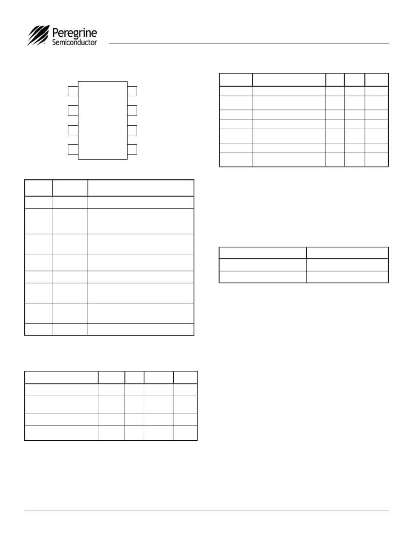
�Figure� 3.� Pin� Configuration� (Top� View)�
�Table� 4.� Absolute� Maximum� Ratings�
�Symbol�
�Parameter/Conditions�
�Min�
�Max�
�Units�
�V� DD�
�1�
�8�
�RF1�
�V� DD�
�Power� supply� voltage�
�-0.3�
�4.0�
�V�
�CTRL�
�GND�
�RFC�
�2�
�3�
�4�
�4230�
�7�
�6�
�5�
�GND�
�GND�
�RF2�
�V� I�
�V� CTRL�
�T� ST�
�T� OP�
�P� IN�
�Voltage� on� any� input�
�except� for� the� CTRL� input�
�Voltage� on� CTRL� input�
�Storage� temperature� range�
�Operating� temperature�
�range�
�Input� power� (50� ?� )�
�-0.3�
�-65�
�-40�
�V� DD� +�
�0.3�
�5.0�
�150�
�85�
�35�
�V�
�V�
�°C�
�°C�
�dBm�
�V� ESD�
�ESD� voltage� (Human� Body�
�Model)�
�250�
�V�
�Table� 2.� Pin� Descriptions�
�Absolute� Maximum� Ratings� are� those� values�
�Pin�
�No.�
�1�
�2�
�3�
�Pin�
�Name�
�V� DD�
�CTRL�
�GND�
�Description�
�Nominal� +3V� supply� connection.�
�CMOS� or� TTL� logic� level:�
�High� =� RFC� to� RF1� signal� path�
�Low� =� RFC� to� RF2� signal� path�
�Ground� connection.� Traces� should� be�
�physically� short� and� connected� to� ground�
�plane� for� best� performance.�
�listed� in� the� above� table.� Exceeding� these� values�
�may� cause� permanent� device� damage.�
�Functional� operation� should� be� restricted� to� the�
�limits� in� the� DC� Electrical� Specifications� table.�
�Exposure� to� absolute� maximum� ratings� for�
�extended� periods� may� affect� device� reliability.�
�Table� 5.� Control� Logic� Truth� Table�
�Control� Voltage�
�Signal� Path�
�4�
�RFC�
�Common� RF� port� for� switch.� 1�
�CTRL� =� CMOS� or� TTL� High�
�RFC� to� RF1�
�5�
�RF2�
�RF2� port.�
�1�
�CTRL� =� CMOS� or� TTL� Low�
�RFC� to� RF2�
�6�
�7�
�8�
�GND�
�GND�
�RF1�
�Ground� Connection.� Traces� should� be�
�physically� short� and� connected� to� ground�
�plane� for� best� performance.�
�Ground� Connection.� Traces� should� be�
�physically� short� and� connected� to� ground�
�plane� for� best� performance.�
�RF1� port.� 1�
�The� control� logic� input� pin� (CTRL)� is� typically�
�driven� by� a� 3-volt� CMOS� logic� level� signal,� and�
�has� a� threshold� of� 50%� of� V� DD� .� For� flexibility� to�
�support� systems� that� have� 5-volt� control� logic� driv-�
�ers,� the� control� logic� input� has� been� designed� to�
�handle� a� 5-volt� logic� HIGH� signal.� (A� minimal� cur-�
�Note� 1:� All� RF� pins� must� be� DC� blocked� with� an� external�
�series� capacitor� or� held� at� 0� V� DC� .�
�Table� 3.� DC� Electrical� Specifications�
�rent� will� be� sourced� out� of� the� V� DD� pin� when� the�
�control� logic� input� voltage� level� exceeds� V� DD� .)�
�Latch-Up� Avoidance�
�Parameter�
�V� DD� Power� Supply� Voltage�
�I� DD� Power� Supply� Current�
�(V� DD� =� 3V,� V� CNTL� =� 3V)�
�Min�
�2.7�
�Typ�
�3.0�
�29�
�Max�
�3.3�
�35�
�Units�
�V�
�μ� A�
�Unlike� conventional� CMOS� devices,� UltraCMOS?�
�devices� are� immune� to� latch-up.�
�Electrostatic� Discharge� (ESD)� Precautions�
�Control� Voltage� High�
�Control� Voltage� Low�
�0.7xV� DD�
�0.3xV� DD�
�V�
�V�
�When� handling� this� UltraCMOS?� device,� observe�
�the� same� precautions� that� you� would� use� with�
�other� ESD-sensitive� devices.� Although� this� device�
�contains� circuitry� to� protect� it� from� damage� due� to�
�ESD,� precautions� should� be� taken� to� avoid�
�exceeding� the� rating� specified� in� Table� 4.�
�?2005� Peregrine� Semiconductor� Corp.� All� rights� reserved.�
�Document� No.� 70-0029-02� │� UltraCMOS?� RFIC� Solutions�
�Page� 2� of� 7�
�Peregrine� products� are� protected� under� one� or� more� of� the� following� U.S.� Patents:� http://patents.psemi.com�
�发布紧急采购,3分钟左右您将得到回复。
相关PDF资料
4231-00
KIT EVAL FOR 4231 RF SWITCH
4237-00
KIT EVAL FOR 4237 RF SWITCH
4239-00
KIT EVAL FOR 4239 RF SWITCH
4242-00
KIT EVAL FOR 4242 RF SWITCH
4244-00
KIT EVAL FOR 4244 RF SWITCH
4245-00
KIT EVAL FOR 4245 RF SWITCH
4246-00
KIT EVAL FOR 4246 RF SWITCH
42551-00
KIT EVAL FOR 42551 RF SWITCH
相关代理商/技术参数
4230-0000LCMD
制造商:3M Electronic Products Division 功能描述:
4230-0000NCMD
制造商:3M Electronic Products Division 功能描述:
4230-0001NCMD
制造商:3M Electronic Products Division 功能描述:
423-0001-01100
制造商:TE Connectivity 功能描述:423-0001-01100
42300-4
制造商:OC White Company 功能描述:MAGNILITE LED MAGNIFIER ESD SAFE 2X 制造商:OC White Company 功能描述:MAGNILITE LED MAGNIFIER ESD SAFE, 2X 制造商:O.C.white 功能描述:Magnilite 6" LED Magnifier with Screw Down Base - 4 Diopter - White 制造商:OC White Company 功能描述:MAGNILITE LED MAGNIFIER ESD SAFE, 2X; Arm Length:43"; Tool Body Material:Aluminium; Magnification:2X; Supply Voltage:240V
423004-000
制造商:TE Connectivity 功能描述:LABEL IDENTIFICATION TAPE
4230043008
制造商:Denon Electronics 功能描述:BELT DCD17/3300
4230044007
制造商:Denon Electronics 功能描述:^4230056008